Mn dopant on the surface of GaAs
Figure 1
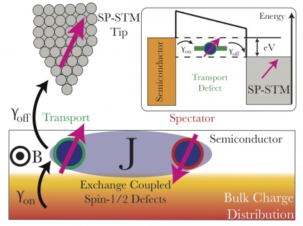
Schematic current path for an electron through a sin- gle dopant (transport site, in green) that is exchange-coupled to another spin-1/2 (spectator site, in red). The transport site has two charge states, empty (spin-0) and full (spin-1/2), and the spectator site’s charge state is stable. These spins reside near the surface of the nonmagnetic host and the Coulomb repulsion at the transport site is assumed to be sufficiently large to prevent double occupation (see inset). Hopping from the transport site to a spin polarized scanning tunneling micro- scope (SP-STM) tip occurs with rate γoff, which is controllable by moving the STM tip relative to the surface. Replenishment of the occupation of the transport site from the nonmagnetic host occurs with a rate γon. If the host is a semiconductor the charge distribution can be adjusted by the STM voltage V through tip induced band bending, which adjusts γon and γoff .
Figure 3
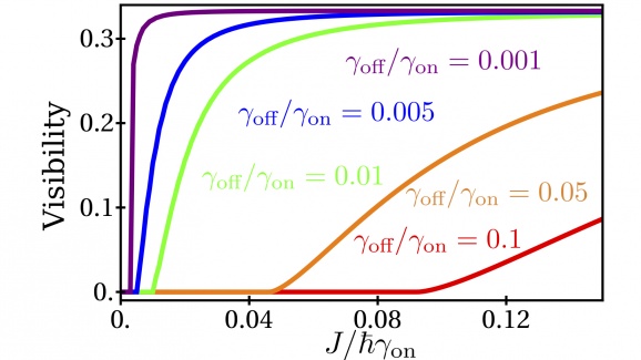
Visibility of the finite-field feature (resonance) as a function of the exchange parameter (J) plotted for different values of the hopping ratio. Smaller hopping ratios yield higher visibility due to extended spin evolution in the exchange field.
Figure 2
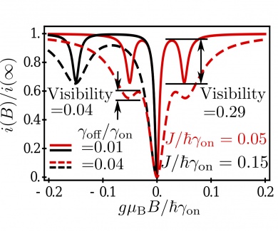
Magnetoresistance of current through spin-1/2 transport dopant for exchange splitting of 0.05 ?γon (red) and 0.15 ?γon (black). Features broaden for moderate extraction rates (dashed) compared to slow extraction (solid).
Figure4
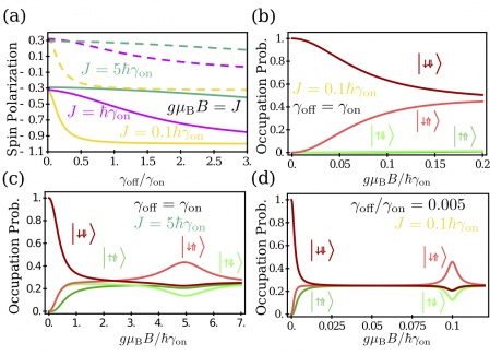
(a) Spin polarization as a function of hopping ra- tio plotted for different values of the exchange coupling. The dashed lines represent the spectator spin and solid lines represent the transport spin. (b-d) Occupation probability for the different states in the product basis as a function of the transverse magnetic field. Shown are (b) γoff = γon, γoff ≫ J, (c)γoff =γon,γoff ≪J,and(d)γon ≫J≫γoff. Good visibility is realized when γoff ≪ J, and especially for (d).